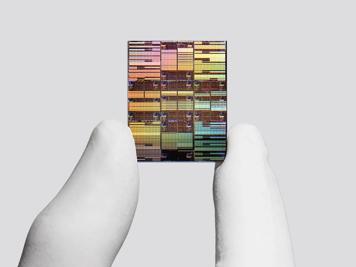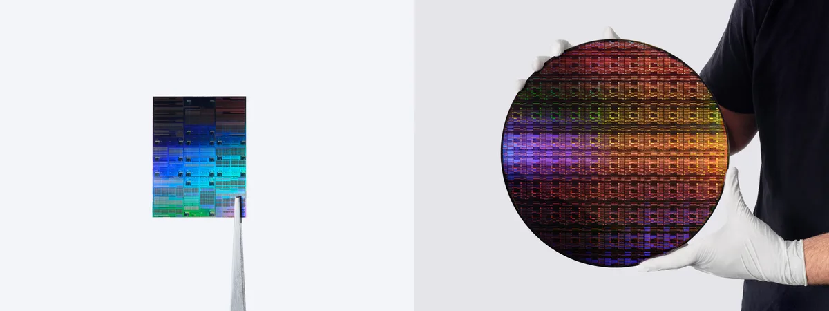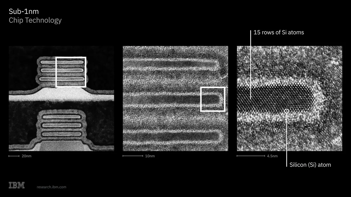
IBM revealed the world's first sub-1 nanometer chip technology featuring a 0.7 nanometer (7 angstrom) transistor architecture on June 25, 2026 [1, 2, 3, 4, 5, 6, 7, 8, 9]. The new chip integrates nearly 100 billion transistors on a fingernail-sized chip, nearly doubling the transistor density of IBM's 2 nanometer chip introduced in 2021 [1, 2, 3, 4, 5, 6, 7, 8, 9].
IBM’s innovation centers around a new transistor architecture called "nanostack," an industry-first design using three-dimensional nanosheet stacks that vertically stagger transistors to increase density [1, 2, 3, 4, 5, 6, 7, 8, 9]. This allows different materials on each transistor layer to optimize performance and power independently [5, 7, 8]. Jay Gambetta, IBM Research Director, said, "With our new nanostack architecture, we’re not just making smaller transistors, we’re reinventing how chips are built to deliver dramatically more power and energy efficiency" [1]. He also added in Chinese, "IBM在芯片领域的最新突破成为了计算技术发展史上的又一个里程碑,将技术从奈米时代推向了原子尺度" [6].
The chip offers up to 50% higher performance or 70% greater energy efficiency compared to IBM’s 2 nanometer node chips [1, 3, 4, 5, 6, 7, 8, 9]. The nanostack design reduces SRAM area by about 40%, enabling more efficient chip layouts suited for AI workloads [5, 8].
IBM expects to begin mass production of the sub-1 nanometer chips within approximately five years, targeting applications in generative AI, cloud infrastructure, and next-generation devices [3, 4, 5, 7, 8, 9]. To support production, IBM plans to introduce high numerical aperture EUV lithography tools and collaborate with equipment manufacturers [8].
This announcement follows Intel's recent unveiling of its 1.8 nanometer chip now in trial production, highlighting industry competition ahead of IBM's volume production timeline [3, 4, 9]. IBM also plans to form a quantum wafer foundry subsidiary named Anderon to provide foundry services, especially in the US [5].