Huawei unveiled the Tau Scaling Law at a semiconductor symposium in Shanghai on May 25, setting a goal to reach transistor density equivalent to the 1.4-nanometre process by 2031 [1, 2, 3, 4]. The new design principle emphasizes reducing the distance and time data travels within chips to boost performance, rather than focusing solely on shrinking transistor size [2, 4].
He Tingbo, chairwoman of Huawei’s Scientist Committee and semiconductor business head, said this approach could "eliminate the need for cutting-edge EUV lithography tools" in achieving these advanced nodes [1, 4]. Huawei plans to apply a related design architecture called LogicFolding in future Kirin chips to shorten wiring length inside chips and enhance efficiency [2, 4].
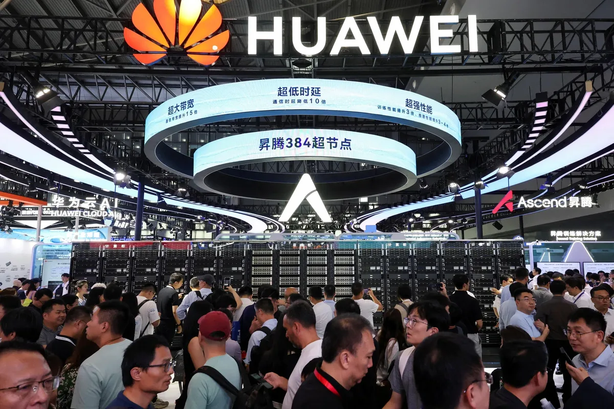
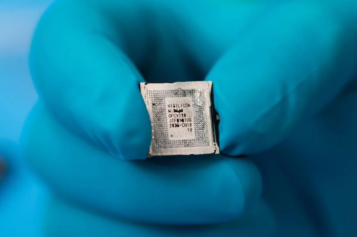
Over the past six years, Huawei has designed and mass-produced 381 chips based on the Tau Scaling Law for applications including artificial intelligence and smartphones [2]. Huawei’s Ascend chip series powers most Chinese AI models, including the DeepSeek flagship model V4 launched in April 2026 [2].
In the broader industry, Taiwan Semiconductor Manufacturing Co (TSMC) currently uses 2-nanometre technology and aims to begin mass production of 1.4-nanometre chips by 2028 [2]. China faces challenges reaching such advanced fabrication levels using conventional methods due to U.S. export controls restricting access to key semiconductor technologies [1, 2, 3]. Gary Ng, a senior economist at Natixis, said, "The US will have less leverage over export control as China becomes more self-sufficient" [1].
Huawei’s announcement energized China’s semiconductor sector, with shares of its chipmaking partner SMIC rising nearly 6% following the news on May 26 [4]. Market confidence was boosted by the scalable design vision Huawei presented.
Huawei aims to achieve the 1.4-nanometre equivalent transistor density within the next five years, targeting 2031 as the milestone completion date [1, 2, 3].